Precision PCB Fabrication, PCB Assembly, DIP Assembly, BGA Assembly etc..
We provide the most competitive PCB & PCBA services.
- All
- Product Name
- Product Keyword
- Product Model
- Product Summary
- Product Description
- Multi Field Search


TVS is a high-efficiency protection device in the form of a diode. After the device is correctly selected, has the design been completed? How to make TVS use the best efficiency in the circuit? The layout and wiring of the printed circuit board is very important. Through the reasonable placement of the TVS, the choice of grounding, the parasitic inductance and the processing of the loop area, the layout and wiring of the PCB can be scientifically and reasonably optimized to optimize the TVS performance.
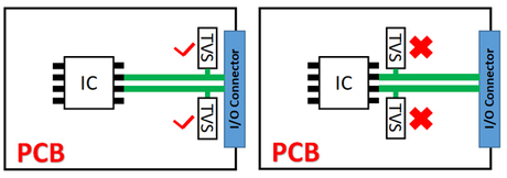
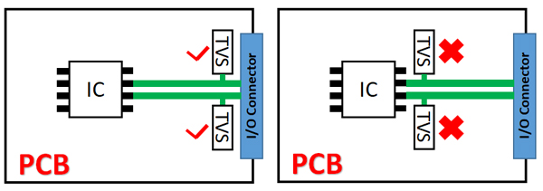
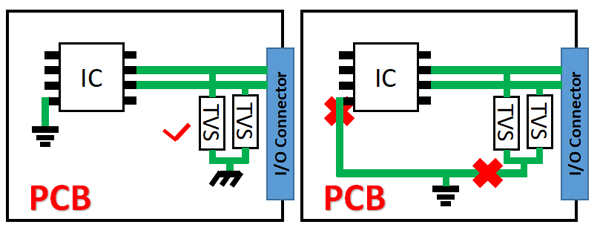
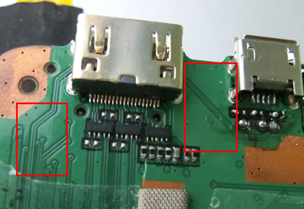
The TVS device is as close to the noise source as possible to ensure that the surge voltage can be clamped before the pulse is coupled to the adjacent PCB wire.
Grounding options
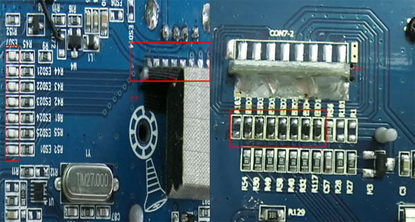
The protection circuit should shunt the surge voltage to the case ground, if shunt the surge voltage directly to the signal ground of the integrated circuit will cause ground bounce. Reducing impedance with relatively short and wide ground leads can improve the clamping performance of TVS diodes on a single ground PCB.
Route selection
TVS wiring should avoid self-inductance. ESD is a sudden pulse of huge change, which may cause parasitic self-inductance in the loop, and then form a strong voltage shock to the loop, and may exceed the IC's tolerance limit and cause damage. The self-inductance voltage generated by the load is proportional to the intensity of the power supply change, and the transient characteristics of ESD shocks are likely to induce high-strength self-inductance.
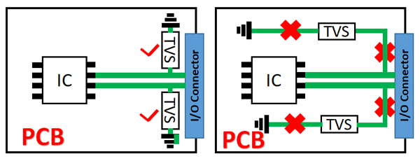
The basic principle of reducing parasitic self-inductance is to shorten the shunt circuit as much as possible. All factors including the ground circuit, the circuit between the TVS and the protected line, and the path from the interface to the TVS must be considered. Therefore, the TVS device should be as close as possible to the interface and as close as possible to the protected line, so as to reduce the chance of self-inductance coupling to other adjacent lines.
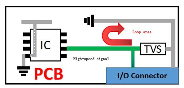
Loop area
Reducing the loop area formed by high-speed data and ground lines can reduce the effects of radiation and radio frequency. Especially when the wire is long, an effective way to alleviate the loop is to include a ground plate in the PCB design to increase the TVS tube to provide isolation for the separation interval between integrated circuits. But it will increase the loop area.
In addition, the following principles can be applied to optimize the line:
1. Try to arrange the interface on the same side;
2. Avoid connecting the protected circuit and the unprotected circuit in parallel, and avoid arrange critical signal lines near the protection circuit;
3. If there are both filtering and protective circuits at the interface, the principle of protection first and filtering second should be followed. The protection circuit is used for external overvoltage and overcurrent suppression. If the protection circuit is placed after the filter circuit, the filter circuit will be damaged by overvoltage and overcurrent.
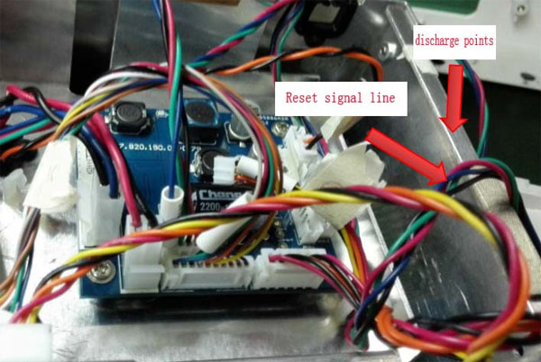
4. Keep reset, interrupt, and control signals away from the input / output ports, and away from the edges and discharge points of the PCB.
Using TVS diodes to implement ESD protection on electronic products is a convenient, effective and highly reliable way. The selection of devices is as important as the PCB layout and wiring. Hope through this brief introduction can help you deepen understanding of the TVS PCB layout design, and do a good job of PCB optimization design in advance, once and for all.